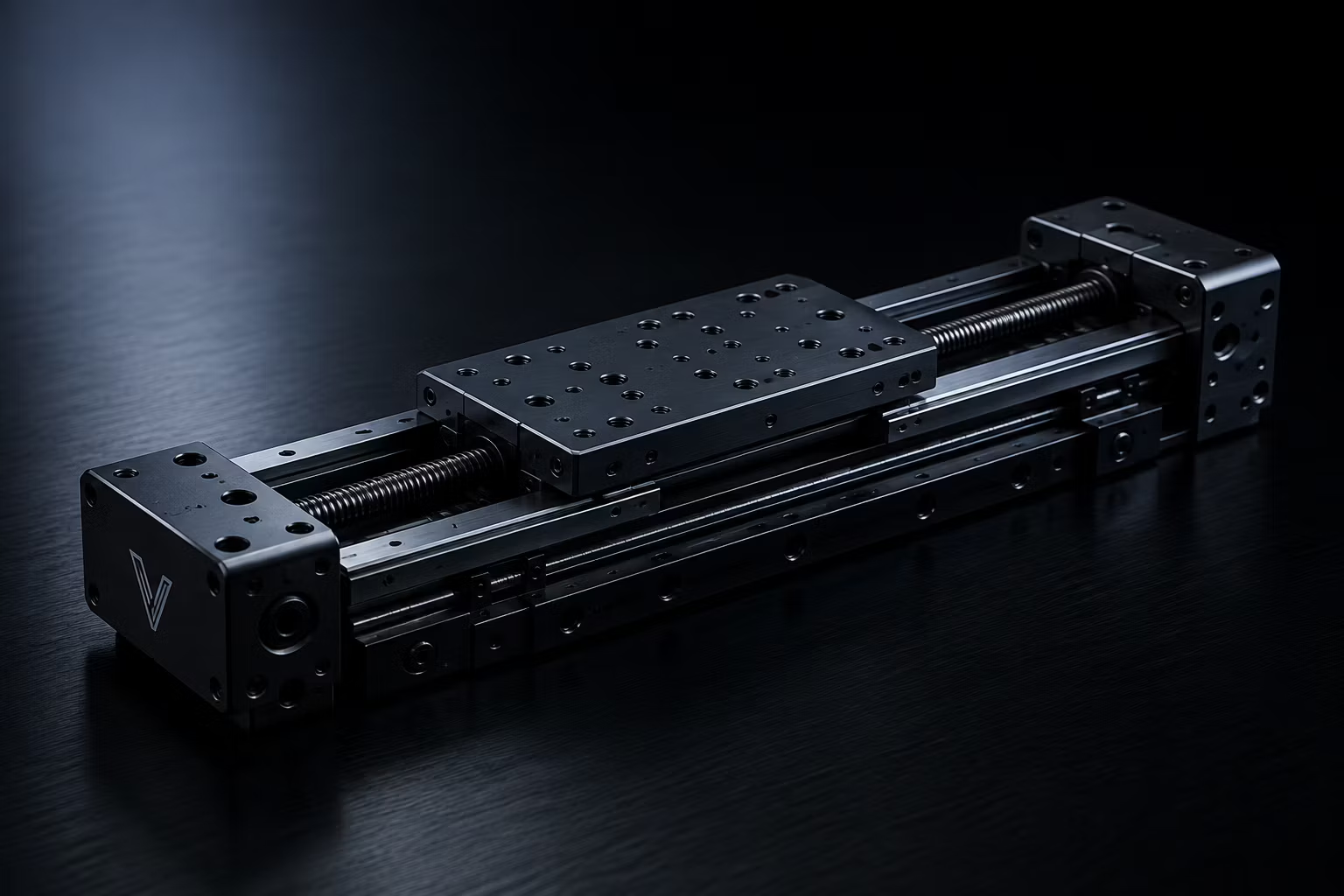
Motion Components
Precision stages, guides, actuators, and rotary modules for controlled semiconductor positioning.
SEMICONDUCTOR
Engineered motion solutions for wafer handling, inspection, metrology, packaging, and precision positioning in advanced semiconductor production.
INDUSTRY OVERVIEW
Semiconductor manufacturing places tight constraints on positioning accuracy, repeatability, contamination control, throughput, and equipment integration.
Vectra Motion develops components, coordinated motion platforms, and automation around those application requirements.
INDUSTRY CHALLENGES
Motion architectures developed around contamination-control and material requirements.
Controlled motion for fine positioning, measurement, and process alignment.
Motion profiles balanced around useful speed, stability, and process control.
Systems engineered around the application’s duty cycle and operating conditions.
RECOMMENDED SOLUTIONS
Precision stages, guides, actuators, and rotary modules for controlled semiconductor positioning.
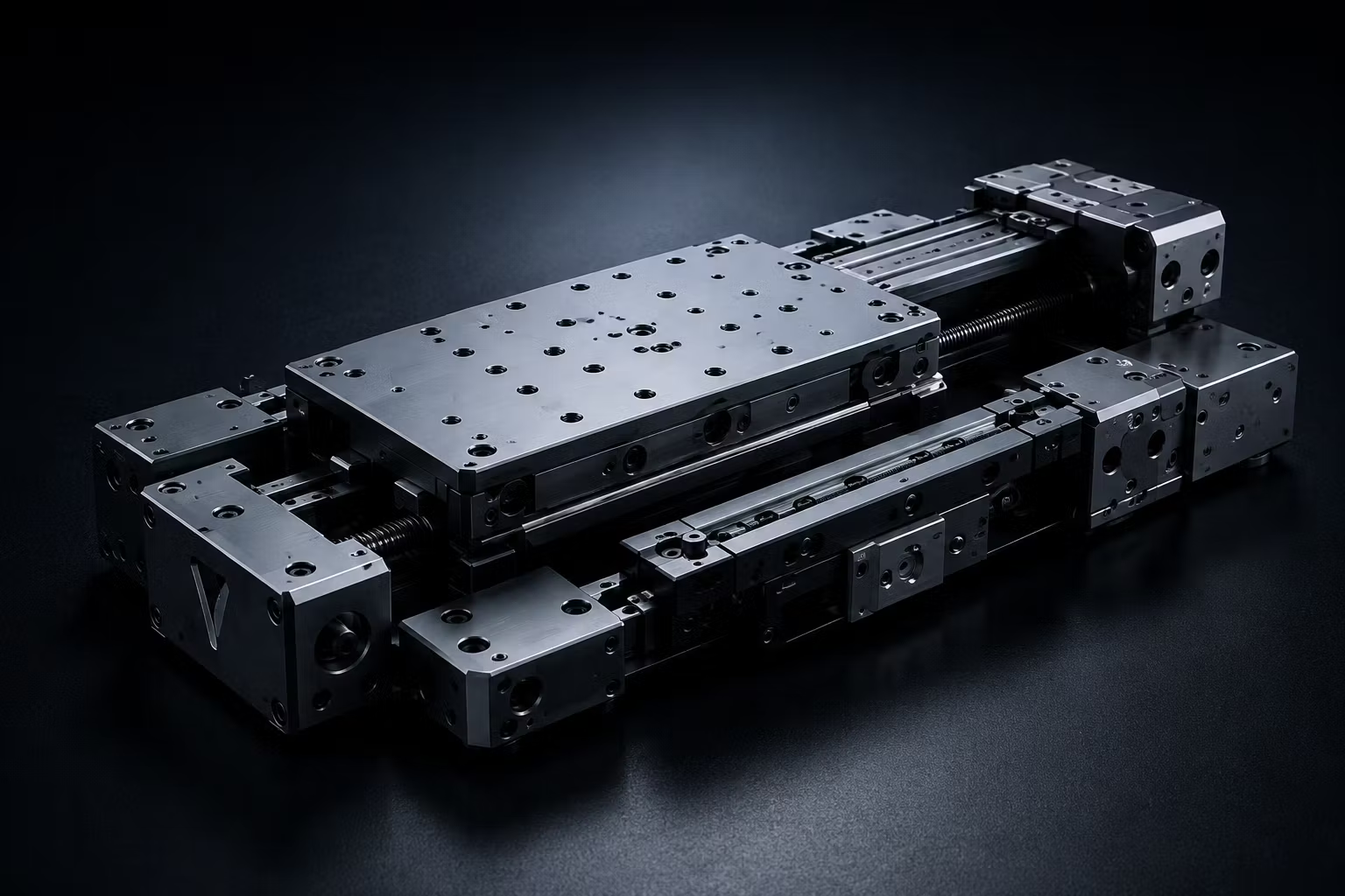
Coordinated multi-axis platforms for wafer handling, inspection, metrology, and process motion.
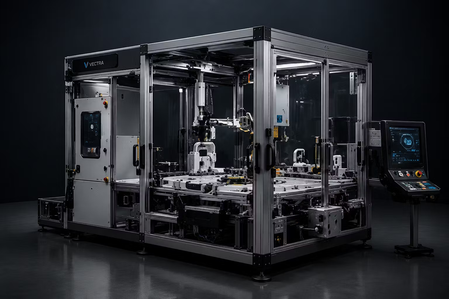
Purpose-built equipment integrating motion, controls, sensing, tooling, and semiconductor workflows.
APPLICATIONS
Controlled transfer, alignment, and positioning.
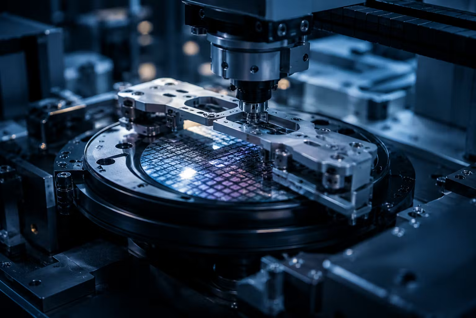
Positioning for measurement and process control.
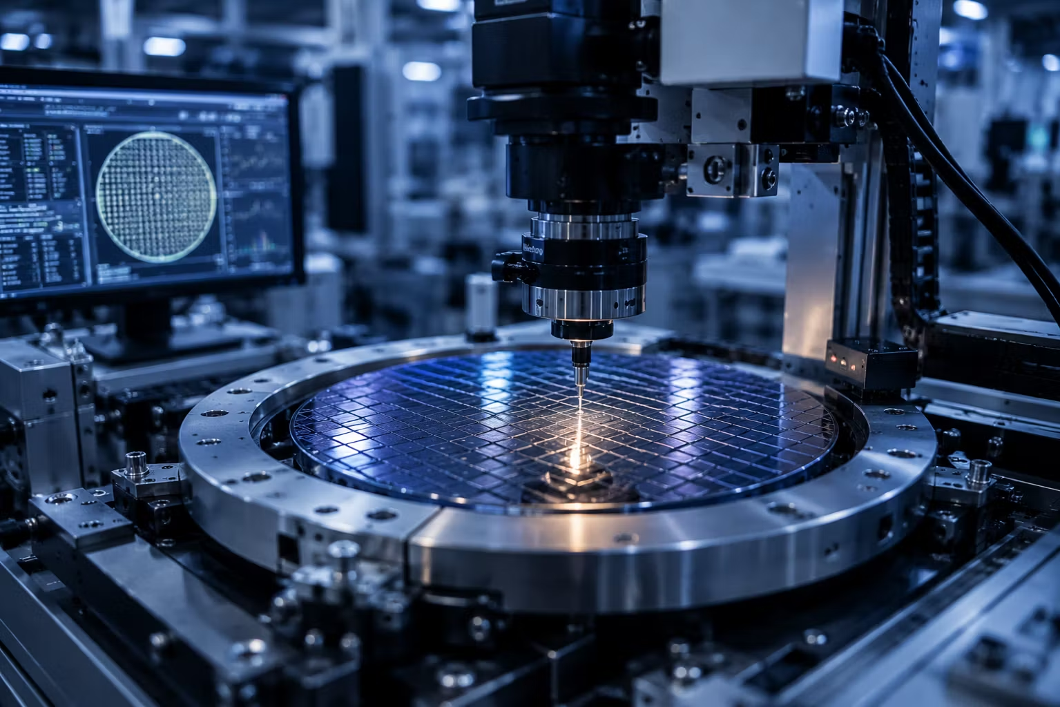
Motion for optical and visual inspection workflows.
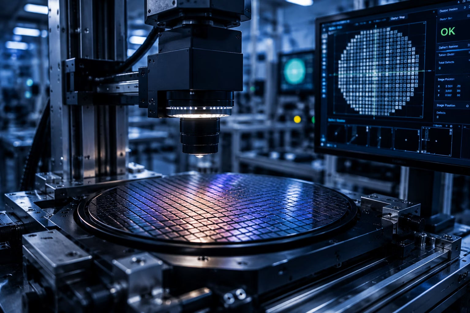
Controlled positioning for patterning equipment.
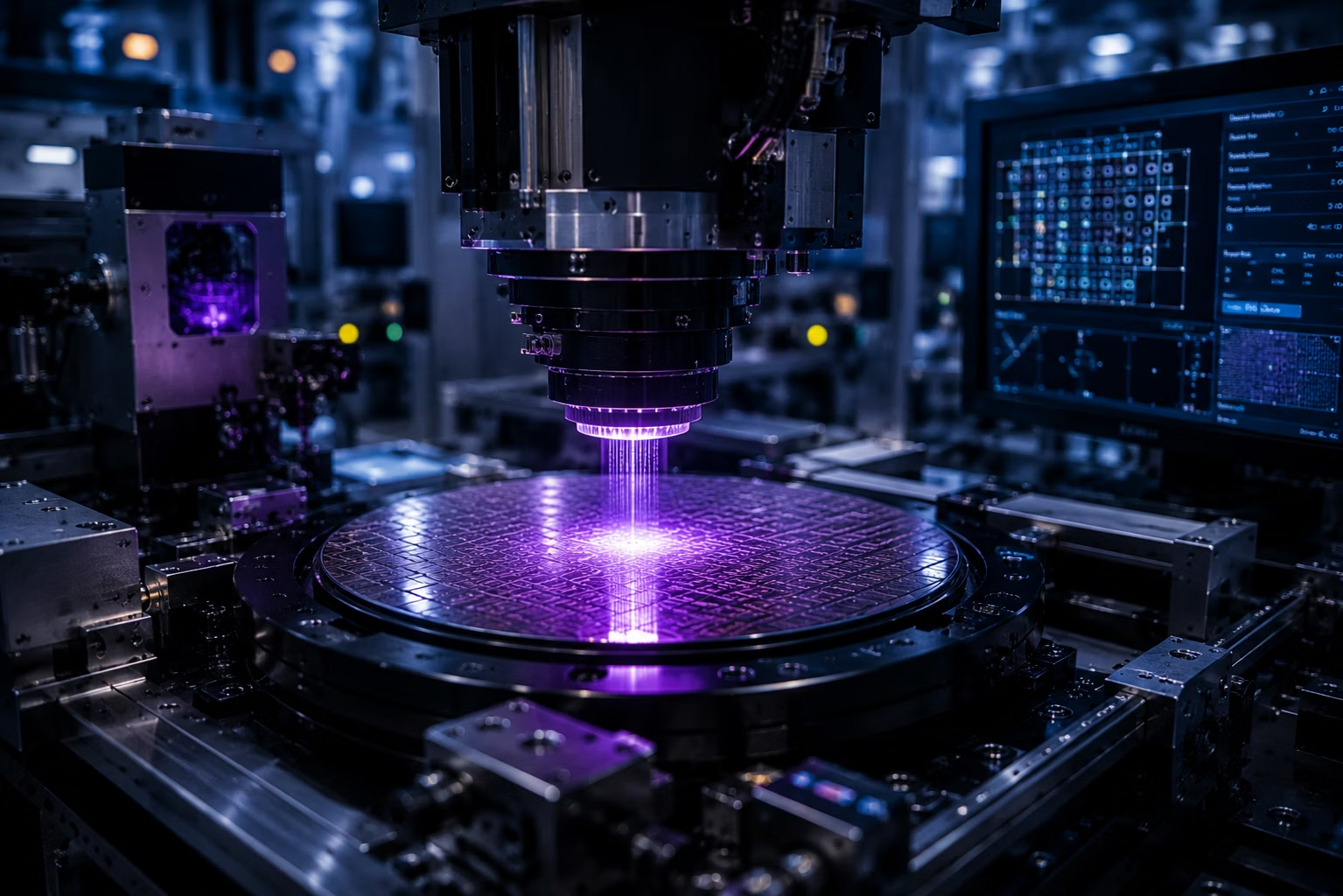
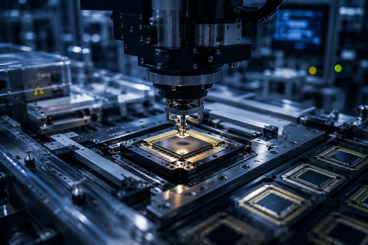
Motion for advanced packaging and final assembly.
APPLICATION EXAMPLE
A precision positioning platform can combine controlled motion profiles, appropriate feedback, and a rigid mechanical architecture to support consistent wafer inspection under defined operating conditions.
Read Case Study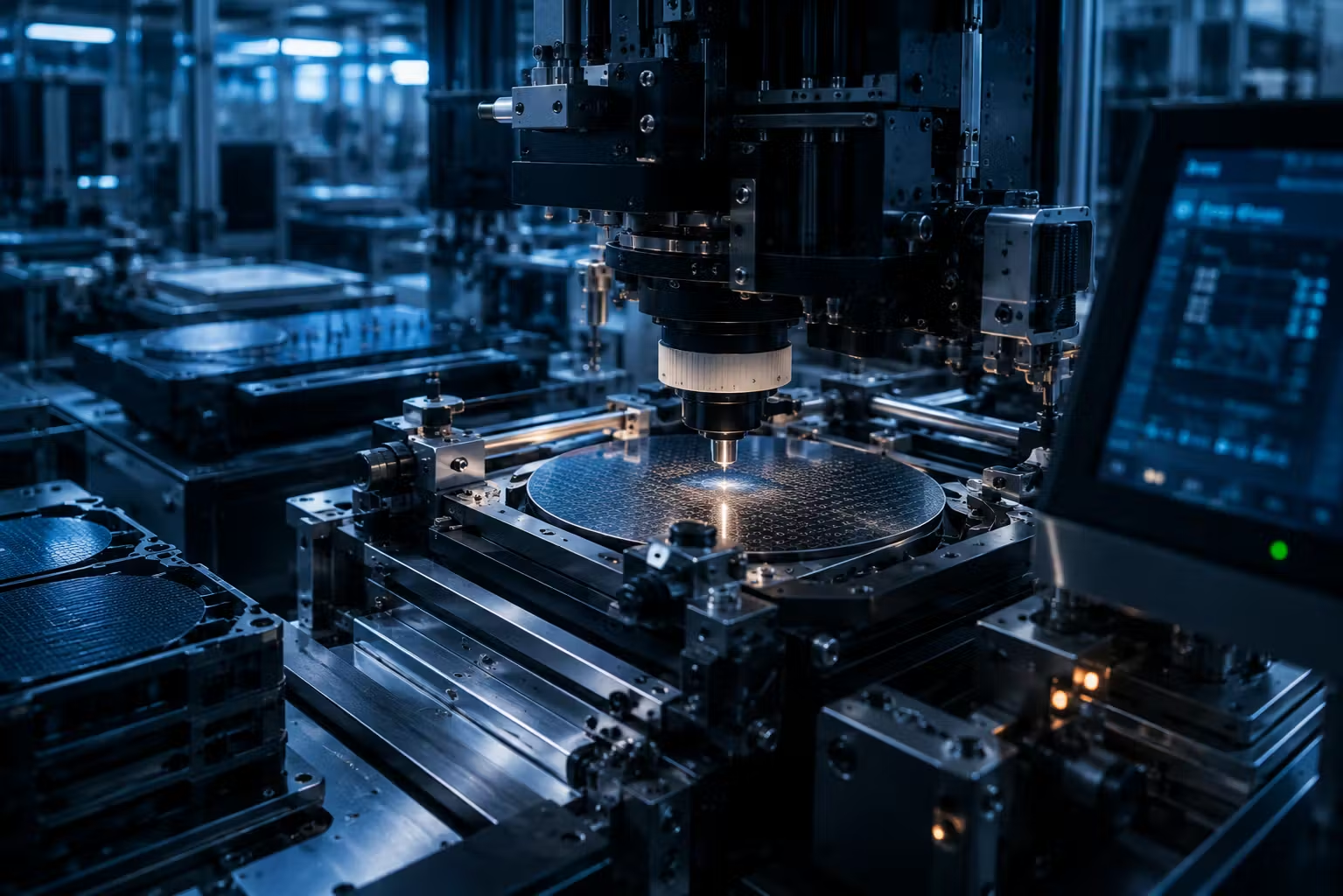
FAQ
Cleanroom suitability depends on materials, lubrication, cable management, particle-generation controls, construction, and the required environmental classification. These constraints are defined during application review.
Systems can be engineered around the required duty cycle, operating conditions, maintenance strategy, and reliability targets. Final performance remains configuration- and application-dependent.
Relevant applications can include wafer handling, inspection, metrology, lithography support, packaging, and precision process positioning where controlled motion is required.
Integration can account for existing controls, tooling, sensing, metrology, safety systems, data interfaces, and material-handling requirements after the interfaces are defined.
Yes. Vectra Motion can combine configurable motion components, coordinated platforms, controls, sensing, and application-specific automation around a defined semiconductor process.
READY TO DISCUSS YOUR APPLICATION?
Share your process, motion, environment, and integration requirements with our engineering team.